


Friendship on Fast Track: Modi & Ishiba Board Shinkansen

Friendship on Fast Track: Modi & Ishiba Board Shinkansen
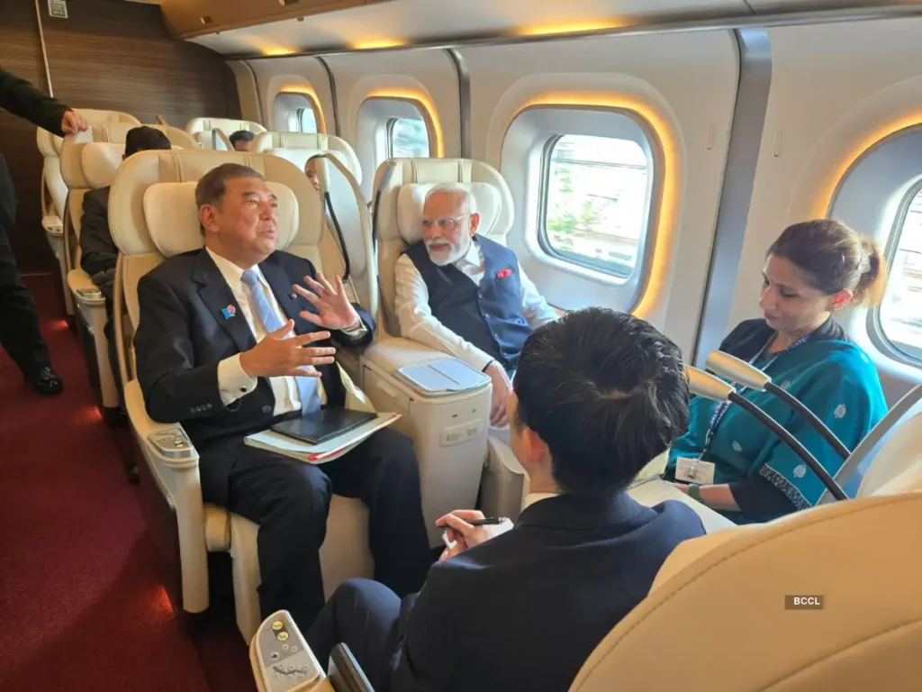
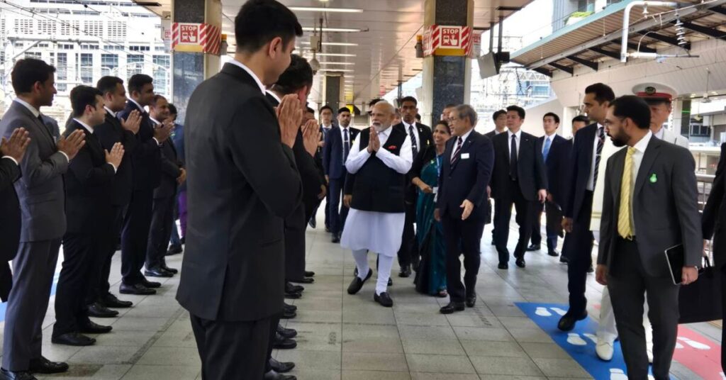
Prime Minister Narendra Modi’s two-day visit to Japan began with a blend of diplomacy and symbolism as he boarded the iconic Shinkansen bullet train alongside his Japanese counterpart, Prime Minister Shigeru Ishiba. The two leaders travelled together to Sendai, with Ishiba personally accompanying Modi throughout the journey.
In a post on X, Ishiba shared: “With Prime Minister Modi to Sendai. Continuing from last night, I will be with you in the car.” The gesture underscored the warmth and camaraderie between the two leaders, reflecting the enduring spirit of India–Japan friendship.
Meeting Indian Train Drivers
Adding to the symbolism, Prime Minister Modi interacted with Indian train drivers currently undergoing training with JR East. The moment was highlighted by Ishiba, who posted images online and called it a proud example of India–Japan collaboration in skill development and technology exchange.
Strategic Talks Beyond Symbolism
Beyond the Shinkansen ride, the two leaders held detailed discussions on strategic areas of cooperation. Key themes included defence, economy, and high-tech collaboration, reflecting the growing depth of the India–Japan partnership.
“We discussed cooperation across a wide range of areas, including defence and the economy. Tomorrow, I will join you for the inspection of the Shinkansen and semiconductor-related matters,”Ishiba wrote on X, signaling the broad agenda of the visit.
Spotlight on Semiconductor Cooperation
The highlight of Prime Minister Modi’s trip to Sendai was his tour of a state-of-the-art semiconductor facility in Miyagi Prefecture. The facility, developed by Taiwan’s Powerchip Semiconductor Manufacturing Corporation (PSMC), SBI Holdings, and Japanese partners under the joint venture Japan Semiconductor Manufacturing Company (JSMC), marks one of Japan’s most ambitious pushes to revive its domestic chip-making industry.
Situated in Ohira Village’s Second Northern Sendai Central Industrial Park, the plant will manufacture 12-inch semiconductor wafers. Production will initially focus on 40-nanometre technology, with plans to expand into 28 nm and 55 nm nodes. A key focus area will be automotive electronics, a sector witnessing massive growth with the rise of electric vehicles and next-generation mobility solutions.
A Boost for Technology and Partnerships
Once fully operational, the Sendai facility is expected to manufacture about 40,000 wafers per month, significantly enhancing Japan’s domestic chip supply. The project also adds momentum to the broader India–Japan technology partnership, aligning with global efforts to diversify semiconductor supply chains and reduce dependency on limited sources.
Prime Minister Modi’s Japan visit not only strengthened diplomatic ties but also showcased how shared technology goals and economic partnerships can shape the future of Asia’s industrial and digital landscape.